In the realm of artificial intelligence, few developments have captured the imagination quite like OpenAI’s ChatGPT. Wit ...
Categories
Post By Date
- May 2026
- April 2026
- March 2026
- February 2026
- January 2026
- December 2025
- November 2025
- October 2025
- September 2025
- August 2025
- July 2025
- June 2025
- May 2025
- April 2025
- March 2025
- February 2025
- January 2025
- December 2024
- November 2024
- October 2024
- September 2024
- August 2024
- July 2024
- June 2024
- April 2024
- March 2024
- February 2024
- January 2024
- December 2023
- November 2023
- October 2023
- September 2023
- August 2023
- July 2023
- June 2023
- May 2023
-
Trends in Cloud Technology
In the realm of technological innovation, cloud technology continues to evolve, captivating hearts and minds alike. With ...
What is Chat-GPT and How powerful it is?
the conversational companion that brings a touch of humanity to our digital interactions. What is Chat GPT?A Conversa ...
3D Mapping using Drones
A journey to the 3D mapping using drones. The latest trend in 3D mapping using drones revolves around enhanced precis ...
-
The Silicon Renaissance of 2026: How EUV...
The semiconductor industry in 2026 is no longer advancing through transistor shrinkage alone. That era—the elegant simp ...
Haven-1 and the Privatization of Microgr...
For more than half a century, microgravity was a geopolitical luxury.Access to orbit belonged to governments, military ...
The Silicon Soul: NVIDIA Jetson Thor and...
The centerpiece of this revolution is the NVIDIA Jetson Thor. Unlike its predecessors, Thor isn't just a processor; it’ ...
Heavy-Duty AI Drones: Force-Controlled X...
For years, drones have hovered on the edge of transforming logistics-promising faster deliveries, reduced human risk, a ...

- Raj
- May 25, 2026
- 5 hours ago
- 2:06 pm
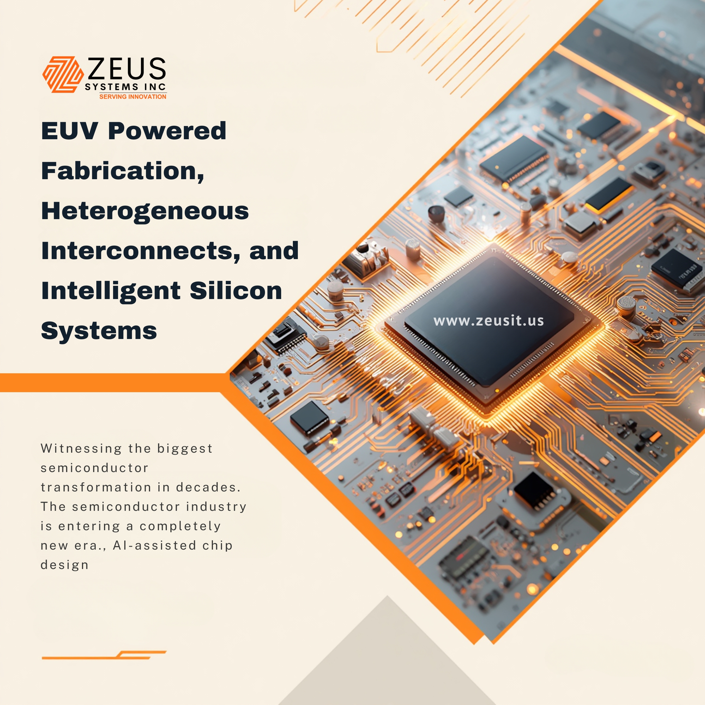
The semiconductor industry in 2026 is no longer advancing through transistor shrinkage alone. That era—the elegant simplicity of Moore’s Law—is dissolving into something far more complex, autonomous, and system-oriented. The modern chip fab is evolving into a computational organism: self-optimizing, AI-assisted, thermally predictive, and deeply interconnected across design, manufacturing, packaging, and runtime orchestration.
At the center of this transformation are three converging revolutions:
- Extreme Ultraviolet (EUV) lithography reaching angstrom-era manufacturing
- AI-assisted Electronic Design Automation (EDA) capable of predictive architecture synthesis
- Heterogeneous interconnect ecosystems enabling composable silicon systems rather than monolithic chips
Together, these technologies are not simply improving semiconductors. They are fundamentally changing what a semiconductor is.
The “chip” of 2026 is no longer a single die.
It is a distributed computational civilization.
The End of Monolithic Thinking
For nearly six decades, chip manufacturing followed a relatively linear philosophy:
• shrink transistors,
• increase density,
• raise clock speeds,
• reduce power per operation.
But by 2026, physical scaling has entered a zone where atomic behavior, quantum variability, thermal instability, and interconnect latency increasingly dominate performance outcomes. Industry leaders openly acknowledge that packaging, interconnects, and system-level co-optimization are now as important as transistor density itself.
The consequence is historic:
Semiconductor innovation has shifted from device scaling to system orchestration.
The modern fab no longer manufactures isolated processors.
It manufactures integrated computational ecosystems.
EUV Lithography Becomes Computational Physics
Extreme Ultraviolet lithography once represented merely a manufacturing breakthrough. In 2026, it has become something closer to computational astrophysics.
At sub-2nm geometries, the behavior of photons, resist materials, stochastic defects, line-edge roughness, and atomic-scale variability create conditions where deterministic manufacturing is no longer possible using traditional methods.
This forced fabs into a radical transition:
manufacturing itself became AI-native.
Advanced computational lithography systems now use machine learning models to:
• predict defect probabilities,
• simulate photon scattering,
• estimate thermal deformation,
• optimize curvilinear masks,
• and dynamically compensate for process drift.
Recent research demonstrates AI-enhanced computational lithography achieving massive acceleration while improving process windows and edge placement accuracy.
ASML’s newest High-NA EUV systems are no longer just precision optics machines—they are cyber-physical intelligence platforms combining optics, software, AI inference, and nanometer-scale feedback loops.
This changes the identity of a fab.
A modern semiconductor plant now resembles:
• an exascale simulation center,
• an autonomous robotics facility,
• a materials science laboratory,
• and an AI supercomputer—
all fused into one infrastructure stack.
AI-Assisted Design Is Replacing Human-Centric Architecture
Historically, chip architecture was a human intellectual exercise constrained by engineering teams and verification cycles.
That model is collapsing.
By 2026, AI-assisted EDA systems can autonomously explore millions of architectural permutations simultaneously.
Instead of engineers manually routing logic paths, AI systems now:
• generate floorplans,
• optimize power delivery networks,
• predict thermal hotspots,
• simulate electromigration risks,
• identify congestion regions,
• and co-design package-aware architectures.
This shift is profound because routing complexity has exploded beyond human intuition.
A modern AI accelerator may contain:
• billions of transistors,
• stacked memory systems,
• optical interconnects,
• hybrid-bonded chiplets,
• vertical power delivery structures,
• and thermal-aware logic placement.
No human team can globally optimize such a system manually.
AI can.
The next frontier is not merely automation.
It is predictive silicon cognition.
Design tools are beginning to infer how chips will behave before they physically exist.
This creates an unprecedented capability:
virtual silicon evolution.
Entire generations of chips can now be simulated, stress-tested, optimized, and behaviorally predicted in digital twin environments before a single wafer is exposed.
The Rise of Predictive Silicon
One of the least discussed revolutions of 2026 is behavioral prediction at fabrication scale.
AI models are increasingly trained not only on design data but also on:
• fab telemetry,
• defect histories,
• thermal variance,
• aging curves,
• workload signatures,
• and packaging stress models.
This allows semiconductor companies to predict:
• lifetime degradation,
• thermal runaway scenarios,
• field reliability,
• manufacturing yield,
• and workload-specific instability.
The implications are staggering.
Future chips may ship with:
• embedded predictive health systems,
• runtime self-optimization engines,
• and adaptive frequency governors trained on manufacturing-origin data.
In essence:
chips are becoming self-aware about their own physical limitations.
This is the beginning of cognitive hardware infrastructure.
Heterogeneous Integration Is the New Moore’s Law
The greatest architectural breakthrough of the decade may not be transistor scaling at all.
It may be heterogeneous interconnect design.
Traditional monolithic SoCs are becoming economically and thermally unsustainable at advanced nodes. Yield losses alone become catastrophic as die size increases.
The industry solution is modular silicon composition:
chiplets.
Instead of one giant processor, future systems combine specialized dies:
• AI accelerators,
• CPUs,
• memory stacks,
• photonics engines,
• networking fabrics,
• analog controllers,
• security enclaves,
• and real-time industrial inference modules—
all interconnected within a single package.
This is heterogeneous integration.
And it is redefining hardware engineering itself.
The New Semiconductor Stack: “Systems on Package”
The future is not SoC.
It is:
SoP — System on Package.
Advanced packaging technologies now allow:
• 2.5D interposers,
• 3D stacking,
• hybrid bonding,
• backside power delivery,
• glass substrates,
• and silicon bridges
to create systems with interconnect density once considered physically impossible.
This means engineers can build architectures never before manufacturable.
Examples emerging in 2026 include:
Industrial Autonomous Control Silicon
Dedicated AI dies tightly coupled with:
• deterministic real-time compute,
• FPGA logic,
• sensor fusion processors,
• and edge inference memory systems.
Self-Healing Robotics Processors
Packages that dynamically reroute workloads around degraded chiplets using AI-guided interconnect management.
Adaptive Factory Compute Meshes
Industrial automation chips capable of workload migration between thermal zones inside the package itself.
Physics-Aware Manufacturing AI
Systems where embedded ML models continuously optimize machine behavior at runtime based on vibration, heat, and predictive maintenance telemetry.
This is not evolutionary computing.
It is silicon urbanization.
Industrial Automation Becomes the Ultimate Semiconductor Customer
Consumer devices once drove semiconductor progress.
Now industrial automation is becoming one of the strongest architectural forcing functions.
Factories increasingly require:
• ultra-low latency inference,
• deterministic AI,
• machine vision,
• edge robotics,
• digital twins,
• predictive maintenance,
• and autonomous coordination.
Traditional CPUs cannot efficiently solve these multidimensional requirements.
Heterogeneous SoPs can.
Future industrial chips may include:
• real-time operating cores,
• AI tensor arrays,
• photonic communication lanes,
• secure enclave dies,
• and thermal-adaptive routing fabrics—
all within a unified package optimized for robotics and autonomous manufacturing.
This creates an entirely new semiconductor category:
industrial cognitive silicon.
AI Is Now Designing the Factory That Designs AI Chips
The recursion here is extraordinary.
AI accelerators are:
• designing next-generation chips,
• optimizing lithography,
• controlling fab robotics,
• predicting failures,
• managing supply chains,
• and orchestrating packaging systems.
In effect:
AI is becoming the operating system of semiconductor manufacturing itself.
Modern fabs increasingly rely on:
• autonomous metrology,
• AI-driven defect classification,
• predictive maintenance,
• robotic wafer handling,
• and self-correcting process optimization.
Industry leaders now describe semiconductor manufacturing as a software-defined production environment rather than a static industrial process.
The Real Bottleneck Is No Longer Transistors
The semiconductor wars of 2026 are not fundamentally about transistor density anymore.
They are about:
• advanced packaging capacity,
• HBM integration,
• thermal management,
• substrate availability,
• power delivery,
• and AI-enabled EDA ecosystems.
Packaging has transformed from a backend commodity into the strategic center of hardware innovation.
This is why companies are investing aggressively in:
• CoWoS,
• silicon interposers,
• chiplet standards,
• hybrid bonding,
• and advanced substrate ecosystems.
The “backend” is becoming the frontend of innovation.
The Geopolitical Consequences
Semiconductors are no longer merely economic assets.
They are civilization infrastructure.
The convergence of:
• AI,
• defense,
• robotics,
• energy systems,
• industrial automation,
• cloud infrastructure,
• and sovereign compute
has transformed fabs into geopolitical power centers.
High-NA EUV tools, advanced packaging capabilities, and AI-enhanced EDA ecosystems are now strategic national assets.
The next global superpowers may not be defined by oil reserves or manufacturing labor.
They may be defined by:
• packaging ecosystems,
• AI-driven fabs,
• and photonic interconnect leadership.
Beyond Moore: The Era of Computational Materials
The deepest shift underway is philosophical.
For decades, chips were viewed as static hardware.
In 2026, semiconductors are evolving into:
• adaptive systems,
• predictive infrastructures,
• composable architectures,
• and software-defined physical intelligence.
Future processors may:
• dynamically reconfigure interconnect paths,
• shift workloads thermally,
• age-aware optimize frequencies,
• and predict failures before they occur.
This dissolves the line between:
• hardware,
• software,
• manufacturing,
• and AI.
The semiconductor industry is no longer building components.
It is building:
living computational substrates.
Conclusion: The Birth of Synthetic Silicon Intelligence
The fabs of 2026 represent the beginning of a new industrial epoch.
EUV lithography has evolved into computational nanophysics.
AI-assisted design has become autonomous architecture exploration.
Heterogeneous interconnects have dissolved the concept of a single chip.
Packaging has become system engineering.
Factories have become AI organisms.
And semiconductors themselves are becoming predictive, adaptive, and increasingly self-optimizing.
The next decade will not simply deliver faster processors.
It will deliver:
• cognitive hardware,
• composable machine intelligence,
• autonomous industrial compute,
• and infrastructure capable of redesigning itself.
The semiconductor industry is no longer shrinking transistors.
It is engineering the nervous system of planetary-scale intelligence.